
|
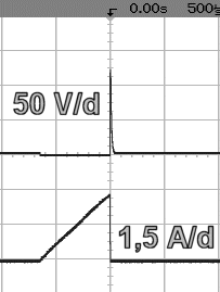
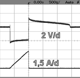
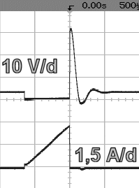
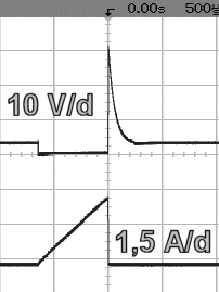
Transient response of semiconductor switches for different types of load |
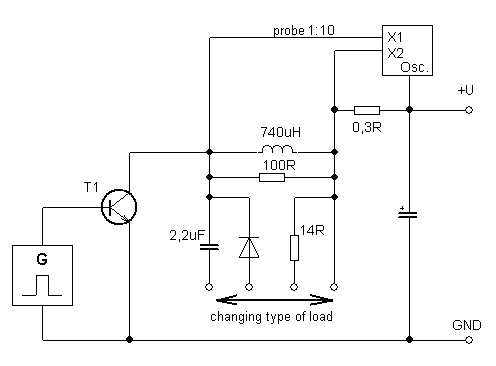
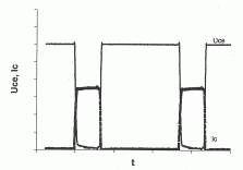
The influence of load on the curves of IC and UCE
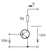
| resistor load (inductance-less) | load with inductors |
 |
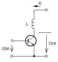 |
| schematic diagram | |
 |
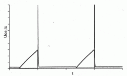 |
| waveform of voltage and current UCE(t), IC(t), time domain | |
 |
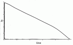 |
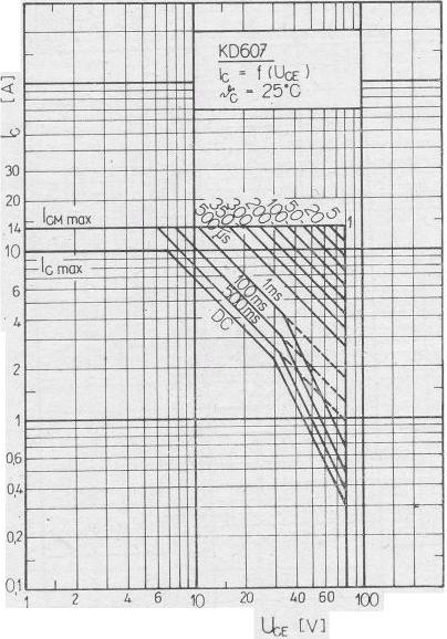
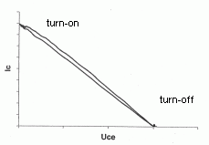
| state diagram, movement of "working point" in the XY area, IC = f (UCE) | |
without snubber circuit |
 with protected diode |
 with damping RC combination |
 with protected diode and resistor |